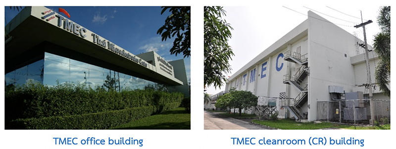
The SMD-1 research team is our of three research teams of Thai Microelectronics Center (TMEC), the organization under the National Electronics and Computer Technology Center (NECTEC) and the National Science and Technology Development Agency (NSTDA), Thailand. The SMD-1 research team provides expertise in research, development, design and engineering (RDDE) of surface innovation and microfluidic, lab-on-a-chip (LOC) and lab-on-a-disc (LOD) devices fabricated by sustainable micro/nanofabrication technology. The services of material characterization and surface analysis are also provided. Additionally, the SMD-1 research team pushes forward TMEC prototypes into commercial products by collaborating with all sectors locally and internationally. The present targets are automated medical screening system with Lab-on-Disc and Large area Super-hydrophobic film for medical and undersea applications.
สารบัญ
Vision
A key partner for research, development, design, and Engineering (RDDE) to develop surface and microfluidic device innovation that is integrated with advanced material characterization and surface analysis for commercialized industrial applications.
Mission
To strengthen research, development, design and engineering (RDDE) and support necessary S&T human resource development (HRD) and technology transfer (TT) with global partners in order to sustainability competitive ecosystem development in Thailand and launch innovation products for global commercialization.
Core Technology
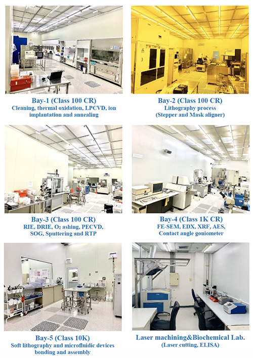
The SMD-1 research team carries out a research activity together with Silicon Industrial Fabrication Research Team (SIFRT) and Design, Simulation, Characterization, and Circuit Design Research Team (DSCRT) by sharing research facilities and utilities at TMEC. The semiconductor devices and all fabrication processes are CMOS compatible fabrication process on 6 inch silicon wafer in class 100 cleanroom.
The main research activities of SMD-1 research team can be categorized into four groups
- Advance lithography process
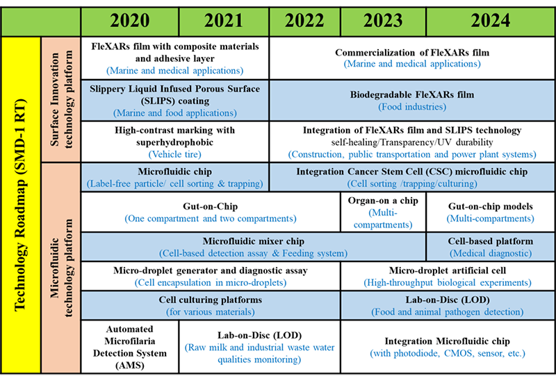
- Surface innovation technology platform
- Microfluidic technology platform
- Advancematerial characterizations and surface analysis
1. Advance Lithography Process
- Photomask design and fabrication
- Thin film deposition (SiO2, Si3N4, Poly-Si, a-Si, TEOS, SOG, Al, Ti, TiN, etc.)
- Chemical etching and plasma etching (RIE and Deep-RIE)
- Silicon mold and intermediate polymer mold fabrication
- Soft lithography process (Polymer micro-structure fabrication)
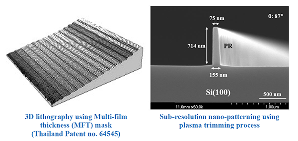
- Sub-resolution patterning (Sidewall Image Transfer (SIT) technology, Photoresist trimming process, and multiple-patterning process)
- 3-D patterning by greyscale lithography and Multi-film thickness mask (MFT-mask)
2. Surface Innovation Technology Platform
- Composite materials with low-surface energy
- Slippery Liquid-Infused Porous Surfaces (SLIPS)
- Frame treatment process (Nano-texturing)
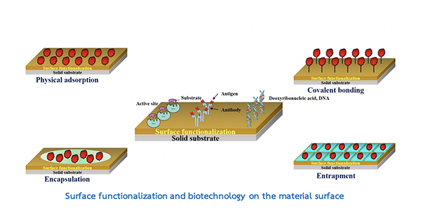
- Surface functionalization
- Molecular analysis
- Superhydrophobic and superoleophobic surface
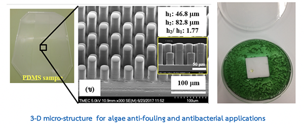
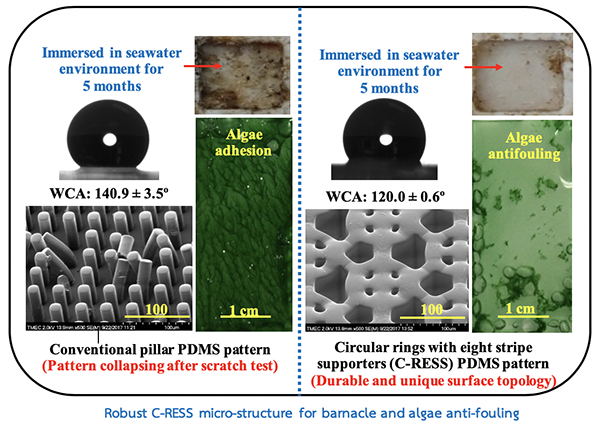
- Anti-bacterial and anti-fouling technologies
- Large-area patterning (R2R and R2P) (collaboration with international partners)
3. Microfluidic technology platform
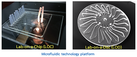
- Microfluidic devices [Lab-on-Chip (LOC), Lab-on-Disc (LOD), Organ-on-Chip (OOC)]
- Micro-droplet devices (cell sorting/cell trapping/cell culturing)
- Plasma bonding and laser cutting
- High-throughput injection molding (collaboration with international partners)
4. Advanced material characterizations and surface analysis
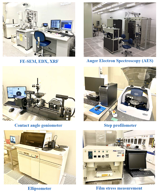
- Field-emission Scanning Electron Microscope (FE-SEM) (with Energy Dispersive X-ray Spectroscopy (EDX) and X-ray Fluorescence (XRF))
- Auger Electron Spectroscopy (AES)
- Contact angle goniometer
- Spectrophotometer
- Ellipsometer
- Film stress measurement
- Step profilometer
Services and consults
- Design, simulation and fabrication of micro/nanostructures by using advance lithography and soft lithography process
- Development of superhydrophobic and superoleophobic surface on various materials
- Design, simulation and fabrication of microfluidic devices, lab-on-a-chip (LOC), lab-on-a-disc (LOD) and Gut-on-a-chip (GOC).
- Advanced material characterization and surface analysis by using Auger Electron Spectroscopy (AES), Field-emission Scanning Electron Microscope (FE-SEM), Energy Dispersive X-ray Spectroscopy (EDX), X-ray Fluorescence (XRF), and Contact angle goniometer
- Tutorial courses on semiconductor technology
Renown Projects
Surface innovation technology platform
1. FleXARs Technology
Large-area flexible polymers with antifouling robust micro-structure for marine, medical, and transportation applications (FleXARs project –an everything-free surface).
2. Slippery Liquid-Infused Porous Surface (SLIPS project)
To produce a large-area antifouling surface for marine & medical applications and public transportation system.
3. High-contrast Marking Vehicle Tire
Ultra-low light reflectivity micro-structure for vehicle and optical devices

Microfluidic Technology Platform
1. Microfluidic Technology Platform
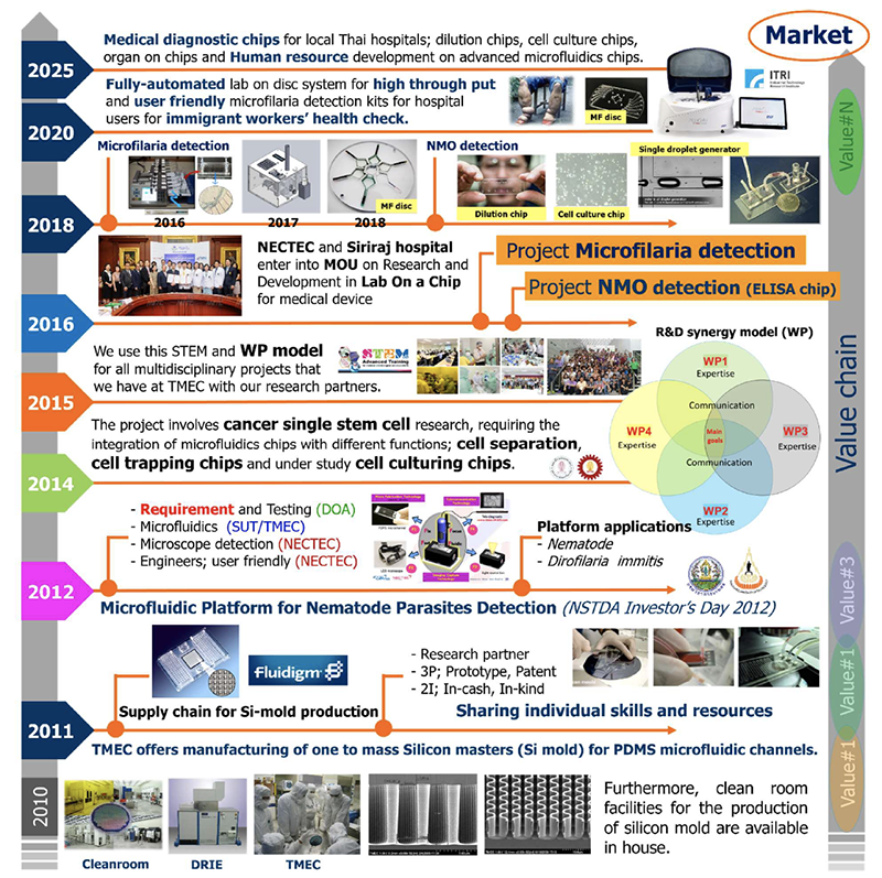
Microfluidic technology platform for cell sorting/cell trapping/cell culturing of cancer stem cell (CSC) and development of micro-droplet generator and diagnostic assay for rapid and high-throughput biological experiments
2. Lab-on-a-Disc (LOD)
Technology platforms of lab-on-a-disc (LOD) for semi-automated Microfilaria detection system (AMS) and LOD for raw milk quality monitoring system
3. Gut-on-a-Chip (GOC)
Technology platform of Gut-on-a-chip based on microfluidics technology for toxicology and pharmacokinetic study of food and pharmaceutical industries and others
Patent lists
- N. Atthi et.al., “Micropallette to holding micro-workpieces by using photolithography process”, Thailand patent (Granted no. 73809), January 2020.
- N. Atthi, et.al., “Chromium/nickel multi-film thickness mask for three-dimensional microstructure fabrication”, Thailand patent (Granted no. 64545), 2018.
- N. Atthi, et.al., “Photoresist 3D structures formation by varying dose technique from a single light source”, Thailand patent (Pending no. 0701001176), March 2007.
- N. Atthi et.al., “Multi-Film Thickness Mask, MFT-Mask”, Thailand patent (Pending no. 0701002029), April 2007.
- N. Atthi, et.al., “Chemical-adhesive protective gloves”, Thailand patent (Pending no. 0801003347), June 2008.
- N. Atthi, et.al., “Self-forming microlens by using a deflection of that film”, Thailand patent (Pending no. 0901001917), April 2009.
- O.Trithaveesak, et.al., “Fabrication of planar chemical reference micro-electrode”, Thailand patent (Pending no. 0901002164), May 2009.
- N. Atthi, et.al., “Biosensor arrays fabricated by thin film layer on silicon opaque substrate”, Thailand patent (Pending no. 0901003142), July 2009.
- N. Atthi, et.al., “Laminating an adhesive film on deep-trench substrate for holding it on a vacuum handling system”, Thailand patent (Pending no. 0901003316), July 2009.
- N. Atthi, et.al., “Increasing a surface roughness with pentagonal and octagonal micro-pattern arrays for superhydrophobic surface”, Thailand patent (Pending no. 0901003706), July 2009.
- J. Supadech, et.al., “Fabrication of water and oil-repellant with a high reflectivity surface by using black silicon”, Thailand patent (Pending no. 1001001270), August 2010.
- N. Atthi, et.al., “Method to make a photoluminescence on silicon nano-pillar”, Thailand patent (Pending no. 1001001708), November 2010.
- K. Saejok, et.al., “Method and process step to make a cavity for silicon surface membrane sensor”, Thailand patent (Pending no. 1101000088), April 2011.
- N. Atthi, et.al., “Increasing the pattern density and surface area by using trimming lithography”, Thailand patent (Pending no. 1101001717), August 2011
- S. Boonruang, et.al., “Sub-diffraction limited diffractive optical elements”, Thailand patent (Pending no. 1201000867), January 2012.
- N. Atthi, et.al., Antifouling Materials and Method of Fabrication Therefor”, Thailand patent (Pending no. 1701003836), July 2016.
- N. Atthi, et.al., “Anti-fouling materials with robust microstructures”, Thailand patent (Pending no. 1801005675), August 2018.
- N. Atthi, et.al., “Anti-fouling materials with robust guard-ring microstructures”, Thailand patent (Pending no. 1801005676), August 2018.
- N. Atthi, et.al., “Antifouling Robust Microstructure”, Thailand patent (Pending no. 1802004081), August 2018.
- N. Atthi, et.al., “Robust Microstructure with Guard Ring Pattern”, Thailand patent (Pending no. 1802004082), August 2018.
- P. Pattamang, et.al., “Lab-on-disc for substance separation and characterization”, Thailand patent (Pending no. 1902004384), November 2019.
- N. Atthi, et.al., “Antifouling Robust Microstructure on Material Surface”, Thailand petty patent (Pending no. 1903002291), September 2019.
- K. Saejok, et.al., “Superhydrophobic Electrical Conductivity Probe”, Thailand petty patent (Pending no. 1903002439), September 2019.
Journal publication lists (Selected)
● Surface innovation and advance lithography technologies
- J. Jantawong, et.al., “The study on 3-D microstructure fabrication with gray-scale lithography technique”, Ladkrabang Eng. J., 25 (2), pp. 42-46 (2007).
- N. Atthi, et.al., “Study of optimization condition for spin coating of the photoresist film on 3 inches wafer by Taguchi design of experiment”, Khon kaen Univ. Res. J., 13 (3), pp. 347-352 (2008).
- N. Atthi, et.al., “3-dimensionals lithography techniques for air bearing surface patterning in hard-disk drive reading/writing head manufacturing”, Khon kaen Univ. Res. J., 13 (3), pp. 353-359 (2008).
- N. Atthi, et.al., “Chemical resistant improvement of natural rubber and nitride gloves by coating with hydrophobic film”, Adv. Mater. Res., 55-57, pp. 741-744 (2008).
- N. Atthi, et.al., “Study of optimization condition for spin coating of the photoresist film on rectangular substrate by Taguchi design of an experiment”, Songklanakarin J. Sci. Technol., 31(3), pp. 331-335 (2009).
- O. Nimittrakoolchai, et.al., “Parameter optimization by using a Taguchi’s method for deposition water-repellent film”, Mineral. Met. Mater. Soc., pp. 1185-1190 (2009).
- N. Atthi, et.al., “An effect of viscosity of coating materials on silicon micro-patterning arrays for superhydrophobic surface”, Adv. Mater. Res., 93-94, pp. 447-450 (2010).
- N. Atthi, et.al., “Improvement of photoresist film coverage on high topology surface with spray coating technique”, J.Microsc. Soc. Thailand, 24 (1), pp. 42-46 (2010).
- N. Atthi, et.al., “An effect of silicon micro-patterning arrays on superhydrophobic surface”, J. Nanosci. Nanotechnol., 11, pp. 1-7 (2011).
- N. Atthi, et.al., “Fabrication of ultra-hydrophobic surface with low reflectance using black silicon nanostructures”, NECTEC Tech. J., (22), pp. 180-185 (2010).
- N. Chathirat, et.al., “A micro-grating sensor for DNA hybridization and antibody HSA-antigen HSA interaction experiments”, Jpn. J. Appl. Phys. 50 (1s2), p. 01BK01 (2010).
- N. Atthi, et.al., “Increasing active surface area to fabricate ultra-hydrophobic surface by using “Black silicon” with Bosch etching process”, J. Nanosci. Nanotechnol, 12, pp. 1-9, (2012).
- N. Atthi, et.al., “Effect of black silicon pillar height on water repellent and surface reflectance”, J. Microsc. Soc.Thailand, 4 (1), pp. 32-35, (2011).
- P. Pholprasit, et.al., “Pattern transfer characterization after double-level lithography for a fabrication of the 3-D AlTiC air bearing surface of the hard disk slider”, Jpn. J. Appl. Phys., 51 (6s), p. 06FF08 (2012).
- N. Atthi, et.al., “Trimming lithography: The alternative technology for sub-resolution and sub-wavelength patterning”, ECTI Trans. Electric. Eng., Electron. Commun.,10 (2), pp. 198-207 (2012).
- N. Siwarakrangsun, et.al., “Fabrication of Multi-level photoresist patterns in one-step lithography by using Cr/Ni Multi-film thickness mask,” Adv. Mater. Res., 658, pp. 93-96 (2013).
- C. Viphavakit, et.al., “Development of integrated microfluidic device for optical flow rate sensing”, J. Circuit Syst. Comp., 22, p. 1340016 (2013).
- C. Viphavakit, et.al., “Realization of a polymer nanowire optical transducer by using the nanoimprint technique”, Appl. Optics. 53 (30), p. 1 (2014).
● Microfluidic technology platform
- Phuakrod, et.al., “Diagnosis of feline filariasis assisted by a novel semi-automated microfluidic device in combination with high resolution melting real-time PCR”, Parasites & Vectors (2019).
- D. Ketpun , et.al., “A Potential Application of Triangular Microwells to Entrap Single Cancer Cells: A Canine Cutaneous Mast Cell Tumor Model” , Micromachines 10, 841 (2019).
- T. Tongmanee, et.al., “Effects of the cell and triangular microwell size on the cell-trapping efficacy and specificity”, J. Mechanical Sci. Technol. 33 (11) pp.5571-5580 (2019).
- T. Suwannaphan, et.al., “Investigation of Leukocyte Viability and Damage in Spiral Microchannel and Contraction-Expansion Array”, Micromachines 10, 772 (2019).
- D. Tantraviwat, et.al., “Highly dispersed porous polydimethylsiloxane for boosting power-generating performance of triboelectric nanogenerators”, Nano Energy (2019).
- P. Inpota, et.al., “Chemiluminescence detection with microfluidics for innovative in situ measurement of unbound cobalt ions in dynamic equilibrium with bound ions in binding study with polyethyleneimine and its functionalized nanoparticles”, Talanta, (2018).
- P. Inpota, et.al., “Microfluidic Analysis with Front-Face Fluorometric Detection for the Determination of Total Inorganic Iodine in Drinking Water”, Jpn. Soc. for Analytical Chem., (2018).
- D. Ketpun, et.al., “The Viability of Single Cancer Cells after Exposure to Hydrodynamic Shear Stresses in a Spiral Microchannel”, Micromachines 9(1), (2017).
- A. Thanormsridetchai, et.al., “Focusing and sorting of multiple-sized beads and cells using low-aspect-ratio spiral microchannels”, J. Mechanical Sci. Technol. 31, (2017).
● Biological technology
- P. Saengdee, et.al., “Surface modification of silicon dioxide, silicon nitride and titanium oxynitride for lactate dehydrogenase immobilization”, Biosens Bioelectron, 67, 134-138 (2015).
- P. Saengdee, et.al., “A silicon nitride ISFET based immunosensor for Ag85B detection of tuberculosis”, Analyst, 141(20), 5767-5775 (2016).
- P. Saengdee, et.al., “Optimization of 3-aminopropyltriethoxysilane functionalization on silicon nitride surface for biomolecule immobilization”, Talanta, 207, 120305 (2020).
Members & Expertise
- Dr. Nithi Atthi (Research Team Leader)
(D. Eng. in Electronics and Applied Physics)Expertise: Si-based semiconductor process technology, 3D High-k/metal gate stacks, micro/nanofabrication, lithography process, materials engineering and antifouling surface - Mr. Witsaroot Sripumkhai (Senior Research Assistant)
(M.Sc. in Nanotechnology)
Expertise: Micro/nano technology, Microfluidic, Lab-on-a-chip, Lab-on-a-disc, Gut-on-a-chip, and antifouling surface - Miss Pattaraluck Pattamang (Research Assistant)
(M.Sc. in Nanotechnology)
Expertise: Micro/nano technology, Microfluidic, Lab-on-a-chip, Lab-on-a-disc, Gut-on-a-chip, and antifouling surface - Miss Oraphan Thongsook (Lab Assistant)
(B.S. in Electronics)
Advanced material characterizations (FE-SEM, EDX, XRF, AES), surface analysis (contact angle goniometer), competence of testing and calibration laboratories - Miss. Rattanawan Meananeatra (Senior Research Assistant)(M. Eng. in Microelectronics Engineering)
Expertise: Si-based semiconductor process technology, micro/nanofabrication, lithography process, sensor technologies - Dr. Pawasuth Saengdee (Post-Doc Researcher)
(Ph.D. in Medical Technology)
Expertise: Surface functionalization, Material characterization, Sensor development (Electrochemical device, Quartz Crystal Microbalance (QCM)), Molecular analysis - Mr. Norabadee Ranron (Assistant Researcher)
(M.S. in Mechanical and Automotive Engineering)
Expertise: Microfluidic, Lab-on-a-chip, Lab-on-a-disc, Gut-on-a-chip - Miss Krynnaras Pankong (Assistant Researcher)
(M.Eng. in Electrical Engineering)
Expertise: Telecommunication system, MIMO system, AutoCAD, MATLAB, LabVIEW, C++ - WARINRAMPAI UAHCHINKUL
Expertise: Nanotechnology, Nanomaterials, FE-SEM, HPLC, AF4, DLS, UV-Vis Spectrophotometer and Contact angle goniometer
Contact
Surface and Microfluidic Device Innovation Research Team (SMD-1RT)
Thai Microelectronics Center (TMEC)
e-mail: tmec-smd@nectec.or.th
Tel.: +(66)-38-857100 ext. 124, 125, 307, 312
Website: https://tmec.nectec.or.th/home/index/lang/eng